一、PLL芯片HMC833


芯片初始化设计流程说明:

//
寄存器详细解析:
//

一、The VCO frequency is counted for Tmmt, the period of a single AutoCal measurement cycle. Tmmt= Txtal*R*2n 0AH [2:0] n ; 02H R ;
二、N is the ratio of the target VCO frequency, fvco, to the frequency of the PD, fpd, where N can
be any rational number supported by the N divider. N=Nint + Nfrac/224。
三、The AutoCal state machine and the data transfers to the internal VCO subsystem SPI (VSPI) run at the rate
of the FSM clock, TFSM, where the FSM clock frequency cannot be greater than 50 MHz. TFSM = Txtal · 2m
四、The expected number of VCO counts, V, is given by V =floor(N * 2n)。
五、The nominal VCO frequency measured, fvcom, is given by fvcom = V*fxtal/(2n*R)。
六、where the worst case measurement error, ferr , is: ferr 约等于 ±fpd/2n+1 。
七、total calibration time。 worst case, is given by Tcal= K*128*TFSM+6*TPD2n+7*20TFSM or Tcal=Txtal*(6*R*2n+(140+128*K)*2m) 。
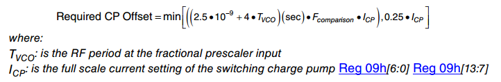
八、The specifc level of charge pump offset current Reg 09h[20:14] is determined by this time offset, the
comparison frequency and the charge pump current:
九、输出频率计算


| 00H | [5]=1 soft reset |
|
|
| 01H | [0]=1 ; no SPI overrides |
|
|
| 02H | This is R; The reference path “R” divider is based on a 14-bit counter and can divide input signals by values from 1 to 16,383 and is controlled by rdiv (Reg 02h) | Minimum pulse width at the reference buffer input is 2.5 ns. For best spur performance when R = 1, the pulse width should be (2.5 ns + 8Tps), where Tps is the period of the VCO at the prescaler input. When R > 1 minimum pulse width is 2.5 ns. |
|
| 05H |
|
|
|
| 06H | [3:2]for DSM mode selection. | [1:0]=2 相位数据是否自动重装选择(推荐值) |
|
|
| [8]AutoSeed 相位数据是否自动重装选择 |
|
|
| 07H | [13] re-Lock 设置 | [3]=1 is a global enable for all lock detect functions. |
|
|
| [6]=1 will result in a variable length lock detect window based upon an internal digital timer. | The timer period is set by the number of cycles of the internal LD clock as programmed by Reg 07h[9:7]. The LD clock frequency is adjustable by Reg 07h[11:10]. |
|
|
| wincnt_max in Reg 07h[2:0] defnes the number of consecutive counts of the divided VCO that must land inside the lock detect window to declare lock. |
|
|
| 08H | [21]The buffer has two modes of operation controlled byReg 08h[21]. High Gain (Reg 08h[21] = 0), recommended below 200 MHz, and High frequency (Reg 08h[21]= 1), for 200 to 350 MHz operation. | [8][9]=1;disable either the pull-up or pull-down sections of the driver [7]=1; keep the SDO driver always on. [6]=1; set “Prevent AutoMux of SDO” [5]=0; disable the driver completely |
|
| 09H | offset charge pump [20:14] | charge pump Down Gain setting[6:0] charge pump Up Gain setting[13:7] |
|
|
| Up Offset select [21]; Down Offset select [22] Offset set [20:14]; |
|
|
| 10H | [7:0] VCO switch ; after every AutoCal operation when changing frequencies. |
|
|
| 11H | [19:0] 实际输出频率与预设频率的误差值 寄存器 | If AutoCal is enabled, (Reg 0Ah[11] = 0), and a new frequency is written, AutoCal will run, but with switches frozen. The VCO frequency error relative to the ommand frequency will be measured and results written to Reg 11h[19:0] where Reg 11h[19] is the sign bit. The result will be written in terms of VCO count error (EQ 4). |
|
| 0AH | [11] AutoCal =1 disabled/=0 enabled | this is m; [14:13] VSCK and AutoCal controller clock = input reference divided by 0,4,16 or 32, set by this reg. |
|
|
| [7:6] this is K The measurement has a programmable number of wait states, k, of 100 FSM cycles | [10] = 1The frequency limits of the VCO can be measured using the BIST features of the AutoCal machine.This is done by setting Reg 0Ah[10]=1 which freezes the VCO switches in one position. |
|
| 0BH | PD_up_en (Reg 0Bh[5]), if 0, masks the PD up output, which prevents the charge pump from pumping up.` PD_dn_en (Reg 0Bh[6]), if 0, masks the PD down output, which prevents the charge pump from pumping down. | PD Force UP Reg 0Bh[9] = 1 and PD Force DN Reg 0Bh[10] = 1 allows the charge pump to be forced up or down respectively. This will force the VCO to the ends to the tuning range which can be useful in test of the VCO. |
|
| 0CH | = fPD/fgcd, wheref gcd = gcd(fVCO,fPD) |
|
|
| 0FH | GPO即SDO 引脚控制寄存器 见datasheet 1.16 |
|
|
|
|
|
|
|
| fractional mode |
|
|
|
| 05H | the VCO SPI reg
| • required for manual control of VCO if Reg 0Ah[11]=1 (AutoCal disabled) • required to change the RF Divider value if needed (“VCO_Reg 02h Biases”) • required to turn on/off the doubler mode if needed (VCO_Reg 03h[0]) |
|
| 06H | [11] Enable the Fractional Mode =1 | [7]=0; Bypass the Modulator circuit |
|
| 03H | this is Nint ; the integer register intg, (only required if the integer part changes) |
|
|
| 04H | this is Nfrac ;the fractional reg | The fractional register write triggers AutoCal if Reg 0Ah[11]=0, and is loaded into the modulator automatically after AutoCal runs. If AutoCal is disabled, Reg 0Ah[11]=1,the fractional frequency change is loaded into the modulator immediately when the register is written with no adjustment to the VCO. |
|
|
|
|
|
|
| interger mode |
|
|
|
| 05H | the VCO SPI reg |
|
|
| 06H | [11] Disable the Fractional Mode =0 | [7]=1; Bypass the Modulator circuit |
|
| 03H | the integer reg | an integer register write triggers AutoCal if Reg 0Ah[11]=0, and is loaded into the prescaler automatically after AutoCal runs. If AutoCal is disabled, Reg 0Ah[11]=1, the integer frequency change is loaded into the prescaler immediately when written with no adjustment to the VCO. | Normally changes to the integer register cause large steps in the VCO frequency, hence the VCO switch settings must be adjusted. AutoCal enabled is the recommended method for integer mode frequency changes. If AutoCal is disabled (Reg 0Ah[11]=1), a priori knowledge of the correct VCO switch setting and the corresponding adjustment to the VCO is required before executing the integer frequency change. |
|
|
|
|
|
| VCO reg | mute function |
|
|
| 01H | [8:0] = 3H (accomplished by writing to Reg 05h = 188h) | This write effectively enables the master enable, and PLL buffer enable, and disables the manual mode RF buffer, divide-by 1, and RF divider of the VCO subsystem, as shown in Figure 27. Although this write disables the manual mode enables of the VCO subsystem, it has no affect on the PLL or VCO subsystem because typically and by default the VCO subsystem is operating in auto mode. |
|
| 02H | [5:0] divider set by 2/4/6.../60/62 25 MHz to 1500MHz |
|
|
| 03H | [2] = 1 (accomplish by writing to PLL Reg 05h= 2218h in doubler mode, and Reg 05h = 2A98h in fundamental mode of the VCO) | [0]=0 enabling the doubler mode |
|
注意:
1、Fxtal匹配50Ω输入电阻,需对地并联一个100Ω的电阻。
2、电荷泵的设置与fpd相关,必须满足关系:CP offset/CP current

///******
在这里我们使用的是Open Mode
///******


写操作:
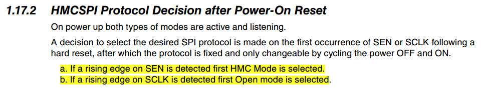
1、上电后先给SCLK一个上升沿,再SEN=1,启动HMC5833的Open Mode。
2、SCLK=0;delay 3ns;SDI=>23bit_data;SCLK=1;delay 3ns开始循环写入24个数据。
3、第24个数据后的SCLK的上升沿时,SEN=0,进入写寄存器地址模式,5bit数据。
4、从第29个数据后,写入3bit的芯片地址(地址为000)。
5、SCLK=1;delay 10ns;SEN=1;delay 10ns;SEN=0;SCLK=0;delay 10ns;


读操作:
1、写入d23-d5个0,d4-d0=register address。
2、r4-r0个0;a2-a0个0.
3、结束写操作。
4、读32个数据。